What is MOSFET-Metal Oxide Semiconductor Field Effect Transistor?
Friday, April 24, 2020
Edit
MOSFET- Metal Oxide Semiconductor Field Effect Transistor
•MOSFET
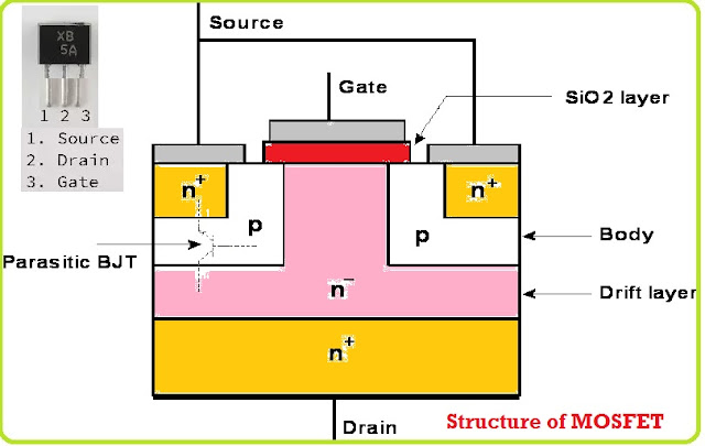
is a three terminal device. The three terminals are source(S), gate (G), drain
(D).It is easy to control by the gate terminal.
•Used
in low-voltage operation where high switching speed is required
•MOSFET
has high blocking voltage capability & improved current carrying capacity.
There
are two types of MOSFET
• n-Channel
MOSFET & P-channel MOSFET
Two modes of operation of MOSFET:
•Gate to source voltage (Vgs) > 0 Enhancement
mode, Conductivity increases with increase in Vgs
•Gate to source voltage (Vgs) < 0 Depletion mode, Conductivity decreases with Vgs
Operation of MOSFET:
Formation of depletion layer
Formation
of Inversion layer
•When Gate is made +ve w.r.t Source.As Vgs is given,
SiO2 layer will act as a capacitor.
• Positive charge is generated on Gate.
• On P type layer negative charge (free electrons) is
generated.
•As Vgs increases , negative charge (free electrons)
also increases.
At the interface, layer of free electrons is referred as the inversion layer which is
shown in below Fig
• Property of inversion layer is same as an n- type
semiconductor.
It is a conductive path or “channel” between the drain and the source which permits flow of current between the drain and the source.
It is a conductive path or “channel” between the drain and the source which permits flow of current between the drain and the source.
Operating
principle of a MOSFET
•Initially there is no current injection
from the gate terminal,since the metal oxide is a very good insulator.
• In MOSFET the gate to silicon oxide(SiO2) layer and the p-body silicon forms
a good quality capacitor.
When a less voltage is applied to this capacitor
structure with gate terminal +ve with respect to the source, a depletion region forms at the interface between
the SiO2 and the silicon.
•The +ve charge induced on the gate metallization
repels the majority hole carriers from the interface region between the gate
oxide and the p type body.
This exposes the negatively charged acceptors
and a depletion region is created.
•Further increase in voltage between gate and source(Vgs) causes the depletion layer to
grow in thickness.
• At the same instant the electric field at the
SiO2-silicon interface gets larger and begins to attract free electrons as
shown in above Fig
•The extra holes are neutralized by electrons from the
source.
Steady state V-I output & Transfer
Characteristics of MOSFET:-
•In the cut-off
mode no drain current flows and
the applied drain–source voltage (Vds) is supported by the body-collector p-n
junction.
•Therefore,
the maximum applied voltage should be below the break down voltage of this
junction (Vdss) to avoid destruction of the device.
•When Vgs is
increased beyond Vgs(threshold) drain
current starts flowing.For small values of voltage between gate to source(Vds), id is proportional to Vds, this mode of operation is called “ohmic mode” of operation.
• Generally MOSFET is operated in the cut off or in the ohmic mode in power electronics applications.
•At high amount of electric field, produced by the high Drain – Source voltage, the drift velocity of free electrons in the
channel tends to saturate.
•As a result the
drain current becomes independent of voltage between drain to source(Vds) and determined by
the gate – source voltage Vgs and this mode is called as active mode of operation of
a MOSFET.


